In many cases, it is necessary to isolate a single defect amidst a vast array of circuitry, singling out a single leaky gate or overdriven transistor from among billions, in order to perform a successful failure analysis. Without some visual way to pluck the single defective device out from the lineup of identical looking circuit elements, an analyst cannot properly target the more destructive steps in the analysis, like cross-section or deprocessing. While some tools, like thermal imaging or other heat-sensitive techniques, can be successful in isolating an area for further investigation, in some cases they aren’t enough; the defect may not be generating enough heat to be detected. In these cases, a different approach, in which one takes the time to understand a device more completely by contrasting some sort of characteristic signature of malfunctioning devices against those that are properly functioning, may be able to isolate the failure. Emission microscopy is one such method of characterizing devices, and offers an excellent picture of many different types of failure upon which to build an analysis.
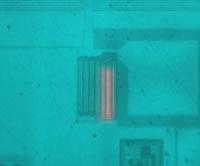
Emission microscopy (often referred to as light emission microscopy, photoemission microscopy, or by the trade name EMMI – EMission MIcroscopy) uses a high-gain camera to detect the infinitesimally small amounts of light emitted by some semiconductor devices and defects. The device under test is placed in a completely dark enclosure that houses the microscope, then is put under electrical bias in the failing condition. The camera system begins acquiring an image (essentially counting photons), mathematically integrating data over times as long as several hours. At the end of the integration time, the system overlays a map of emitted light on top of an image of the failing chip, showing areas of dense photoemission with brightly contrasting bursts of color.
There can be several different causes of photoemission: transistors that have been damaged by electrical overstress or those with gate oxide pinholes, for example, will often photoemit. To confuse things further, there are some semiconductor devices that photoemit even when operating properly, simply as part of their normal operation; aside from the obvious example of optoelectronics like LEDs, memories will often photoemit when being read or written. While it may seem like emission microscopy has the potential to offer false positives, limiting its utility as an analytical tool, it is actually its ability to provide a sort of functional map of a device that makes it so useful.
While emission microscopy can certainly be used successfully to locate many of the same types of defects that can be found with thermally-sensitive techniques – the damaged diffusions that result from an electrical overstress event at an ESD protection diode, for example, is often a great photoemitter – the real benefit comes from the ability to analyze a failing unit with respect to a known good device. By first analyzing a functional device in its normal operating condition, an analyst can generate a reference against which to judge the failing device. With a photoemission image of the reference device in hand, emission microscopy analysis of the failing unit is reduced to a childhood game of “find the differences”, with malfunctioning transistors and damaged diffusions standing in for the typical whimsical fare of tulips or buttons. Another benefit of emission microscopy is that it opens up an alternative method for analyzing very dense, cutting-edge chips, simply by virtue of the nature of the camera used to acquire photoemission images.
Typically, emission microscopy is performed following the chemical decapsulation of a part, after the plastic encapsulant material has been dissolved away from the microchip that lies at the heart of the packaged device. In more modern semiconductor devices, the junctions and transistors of the device (the most likely sources of photoemission) are buried beneath multiple layers of densely packed metal, hiding potential emission sites from the view of the camera. Fortunately, due to the emission microscope camera’s sensitivity to short-wave infrared light, there is a way to image a failing device and completely bypass the problem of the interceding metal layers – by imaging through the back side of the device. First, the device is thinned and polished to a mirror finish, to help facilitate the transmission of photons through the silicon substrate. Because silicon is moderately transparent to infrared light, some photoemission makes it all the way through the substrate and is gathered by the camera; when used in conjunction with a source of infrared illumination, the emission microscope can generate images that are very similar to those taken conventionally, from the top side of the device. By imaging from the back side, the dense metallization that shrouds the emission sites from the camera can be removed from the equation; the active layer is, from the camera’s point of view, the uppermost layer, with nothing but semitransparent silicon substrate in between to intercede.
Emission microscopy can be an invaluable tool for rooting out defects on a failing semiconductor device. It is important to remember, however, that the emission microscope only generates a picture; it is the job of a well-trained failure analyst to take that picture and translate it into data that can be used to root out defects on a malfunctioning device.


