Continued from A Study in Printed Circuit Board Failure Analysis, Part 1
The next step in the failure analysis process, revealing the defect, would almost certainly involve the destruction of the board; as a result, a strong hypothesis was necessary before embarking upon any further analysis. In order to determine the best course of action, our analyst reviewed the facts as they stood before proceeding.
- The failure can be thermally modulated – as board temperature increases, the failure becomes more pronounced.
- In the failing condition, high resistance is measured between two points on the same node. This high resistance results in reduced output current.
- No signs of solder quality issues – cracking or non-wetting – were noted in the area of the failure.
- X-Ray inspection did not reveal any signs of damage to the copper trace between the two suspect points.
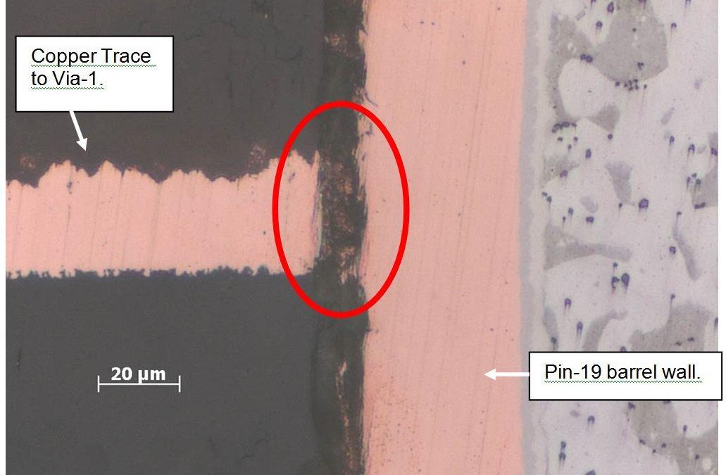
Given this list of facts, our analyst determined that the most likely cause of failure was an intermittent contact between the two points in question that became worse under thermal expansion (as the board materials heated and expanded, less material remained in contact to conduct electricity). The most likely location for this type of failure would be at the connection between the copper trace and the barrel of a via or plated thru-hole; given this hypothesis, the analyst elected to cross-section through the PTH for the suspect pin.
The area of interest was cut away from the bulk of the PCB and encapsulated in epoxy. A cross-section was performed by grinding into the suspect pin with progressively finer grits of polishing abrasive, finishing with a sub-micron polishing compound to bring the sample surface to a finish suitable for high magnification imaging. The PTH was imaged with a high power optical microscope; as hypothesized, an incomplete connection between the copper trace and the PTH barrel was noted (reference figures 5 and 6). The analyst had the proverbial smoking gun; now, the only remaining step was to tie the physical defect to its most likely cause.
Though the physical defect had been revealed, the analyst’s job was not over; the goal of any failure analysis project is to find the root cause of failure and determine the most likely origin of an existing defect. Of the many possible explanations for this type of failure, two were considered as the most likely candidates:
- Mechanical stresses (vibration, thermal cycling, board flexure) may have broken a trace that was originally well connected
- Insufficient etchback or smear removal (followup after drilling holes in the board) was performed during the PCB manufacturing process, preventing a good bond between the buried traces and the barrel
If mechanical stresses were the root cause of this failure, an analyst would expect to see much more damage to the PCB’s copper traces (some degree of tearing or other stress-related cracking); other than the separation from the barrel wall, no such damage was noted. Improper cleaning and etchback during manufacturing, on the other hand, could very well result in an incomplete bond between a buried trace and the via barrel. The defect was therefore classified as most likely occurring during manufacturing. Corrective action was implemented by adding additional inspection and destructive physical analysis on incoming PCBs per IPC-A-600 as part of production screening; as a result, other failures similar to this were found before reaching the end user, and the PCB manufacturer was able to identify and correct an inadequacy in their process.
Conclusion
In this case study, we examined how the failure analysis process enables a defective part to produce actionable data that suppliers and manufacturers can use to improve their product. Despite starting with little more than a nebulous problem description – “this doesn’t work” – the analyst was able to methodically work towards a more comprehensive explanation of the failure; in doing so, an expensive chunk of scrap was transformed into a valuable source of knowledge, identifying a process weakness and helping to prevent further defective product from reaching end users. Future columns will continue to provide other approaches to failure analysis of printed circuit boards (PCB), components, and other electronic devices; in the meantime, keep an open mind, and remember that failure is nothing more than an opportunity to improve!


