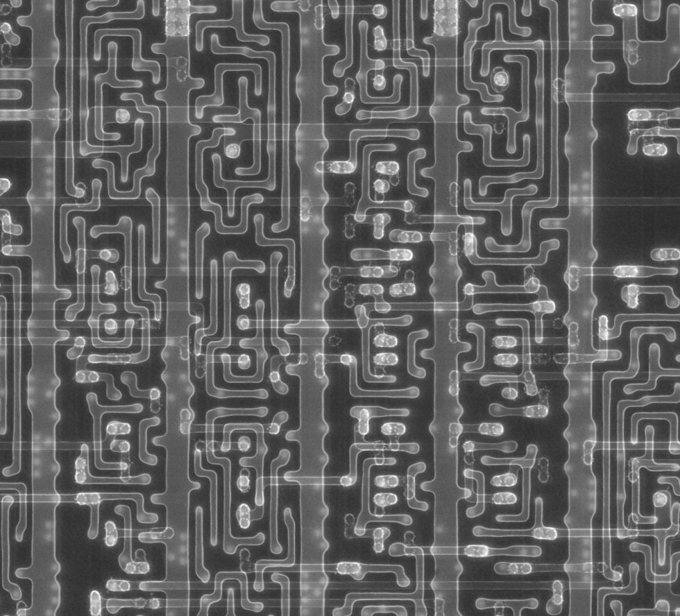
The modern electronics and semiconductor markets are fiercely competitive. Manufacturers are constantly vying for supremacy, attempting to carve out a niche with novel, innovative approaches to fulfill the needs and wants of an increasingly demanding customer base. In such a rapidly changing, fast-paced environment, bringing a new product to market can be challenging, especially without any sort of knowledge of how the competition might measure up. Often, a manufacturer looking to break into the market will employ a third party to perform a technical competitive analysis – an in-depth look at the construction of a product that can provide insight into key details like process node, die size, and functional block size that can be used to perform cost and performance analyses. At first blush, technical competitive analyses appear completely separate from failure analysis services; in reality, the tools and techniques developed for finding defects on cutting-edge products translate seamlessly to the type of teardowns necessary to perform a deep dive into the minutiae of a product’s construction.
In performing failure analysis, the ability to produce the perfect image of a defect is paramount; a crisp, clear photograph of a gate oxide pinhole or metal over-etch can provide a wealth of information to an engineer grappling with catastrophically low yields. Similarly, the right picture is worth a thousand trite clichés when performing a technical competitive analysis. With the same high resolution tools that a failure analyst uses to capture images of melted silicon and metal in the aftermath of an electrical overstress event, it is possible to identify functional blocks on a die, measure the size of a memory cell, and determine the processes used to manufacture a product. High magnification optical images of a product can provide easy-to-interpret, high-level information about a device, while ultra-high resolution electron microscopy can be used to perform circuit extraction, reverse engineering, and process analysis. Of course, just as with failure analysis, there is often a rocky path that must be traversed in order to get to the perfect picture; the sample preparation of a device is just as crucial as the imaging process.
One of the mainstays of the failure analysis process is deprocessing, the act of removing the layers of metal and oxide comprising a device in order to reveal the defects hidden therein. These same techniques are also applicable to technical competitive analysis: in many cases, features of interest are hidden from view (either intentionally or as a consequence of the dense layers of interconnect required in cutting-edge semiconductor products), and must be revealed before any meaningful insight can be gleaned. In many cases, simply removing the metal interconnects to expose the underlying transistors at the polysilicon layer of a device is sufficient; information about functional blocks and process node are easily accessed without the interceding metals obscuring important features. For more in-depth reverse engineering and circuit extraction work, a more methodical, layer-by-layer approach is necessary, so that an expert might be able to trace a signal of interest as it weaves its way through the metallic highways and byways of a circuit. This analytical path is highly targeted towards developing understanding of a device’s circuitry; in order to better understand its construction, other techniques are more suited.
In the same way that cross-sectional analysis is used to view the many layers of an integrated circuit and look for defects or process weaknesses between vertically stacked traces, a cross-section for technical competitive analysis can reveal aspects of a device’s construction that are not readily apparent through deprocessing. The materials used in constructing a device are often equally important as the device’s circuit layout: dielectric composition, the spacing between traces, and the type of metallization used can all greatly impact a device’s performance. Cross-section is also one of the best ways to determine transistor construction characteristics – not just gate length for assessing process node, but atypical transistor constructions that might not be readily apparent from a top-down inspection (for example, the appearance of LDMOS in an RF block of a baseband processor). With the proper sample preparation, an expert can even make inferences about dopant types and profiles based on a cross-sectional inspection.
A very close cousin of technical competitive analysis is intellectual property investigation – specifically, patent infringement analysis. As mentioned, the modern electronics and semiconductor markets are fiercely competitive; so competitive, in fact, that safeguarding one’s intellectual property in order to maintain a technological edge is crucial. Using the same set of aforementioned techniques, a team of analysts can generate a compelling dataset to prove infringement on a client’s IP; in doing so, the client can maneuver themselves into a position of strength for licensing negotiations or IP litigation.


