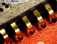
A failure analysis lab employs a wide variety of techniques to search for defects in integrated circuits. Last week, we had seen what goes on inside a failure analysis lab and today we’ll take a look at the different types of printed circuits defects and what class of methods are used to analyze them. It should be noted that any printed circuits defects analysis is preceded by a thorough examination of the facts accompanying the detection of the failure and only after the engineers know what they’re looking for, do they settle down to apply specific failure analysis techniques.
Types of Printed Circuit Board Defects
There are three types of broad defects which can occur in printed circuit boards. Physical disruptions in the material, flaws in the makeup of the material and electrical construction problems. Each of these requires a different approach in detection and shows different symptoms which can be uncovered by analyzing the circumstances surrounding the failure.
Physical disruptions in the material are the most obvious. Not that they’re easy to detect, but they’re easiest for a layman to understand. They occur when the integrity of the chip breaks down in some places. Fatigue cracks and corrosion are two examples of this type of breakdown. Frequently, the defects are tiny and can’t be seen without assistive technologies.
Dye penetrant testing is an excellent way to detect these failures. The chip is stained with a coloring material that reveals cracks and faults. The specific characteristics of these faults give engineers a clue as to what type of fault it is.
The second type of flaw is one which deals with the purity of the materials. Semiconductor materials are manufactured to very precise specifications with just the correct amount of trace minerals necessary for certain properties. Deviations from this will cause the chip to behave in unexpected ways. Since the deviations can be tiny, precise measurements using various emission techniques are used to determine the extent of the flaws.
The third type of flaw deals with the many electrical faults that can occur on the millions of connections on any given chip. It’s remarkably difficult to detect these flaws, but one of the starting points is to figure out which portion of the chip is overheating. Fluorescent imaging, as well as liquid crystal imaging, can be used to find out where the heat is being generated, though this doesn’t automatically mean that the flaw is present in that area as it could occur somewhere “up river.”
Printed circuits defects require a thorough understanding of how chips work. It’s an exact science as well as an art – and one in which new methods are constantly being innovated.


