Electron microscopy services can provide key data for many types of intellectual property (IP) analysis including patent research, reverse engineering, and microelectronics IP infringement analysis, to name just a few. This post explores how electron microscopy supports electronics intellectual property analysis.
Today’s cutting-edge microelectronics are twisting, labyrinthine networks of nanotechnology, with layers upon layers of intertwined metallic and crystalline structures.
Gone are the days when one could put an electronic device under an optical microscope and, over the course of a few hours, sketch out a relatively accurate functional schematic; the process technology used in creating a modern microprocessor or memory device creates features so small that they are physically impossible to resolve with optical microscopy since the wavelength of visible light is so much larger than the features being imaged.
Higher-resolution electron microscopes can easily resolve the nanometer-scale features on these devices, but the ultra-high magnifications needed to do so mean that only very small areas of the die can be viewed at a given time, an equally restrictive roadblock to understanding a circuit as a whole.
Intellectual Property Analysis of Electronics
Performing intellectual property analysis on an electronic device in order to protect patents or reverse engineer obsolete electronic parts which are no longer manufactured is, in many cases, an exercise in competing compromises; one can get a highly focused analysis with electron microscopy that is very limited in scope, or a very broad look at a device that may lack the necessary depth for certain investigations.
Fortunately, Spirit is offering electron microscopy services that work to bridge the gap between viewing large areas and imaging at high resolution.
The Higher the Resolution the Better for Intellectual Property Analysis
When performing intellectual property analysis on electronics to determine whether or not there is patent infringement, it is often important to closely study the materials and processes used to construct a specific semiconductor, integrated circuit, or other devices.
The minutiae of how a transistor is formed can be crucial to the claims of a given electronic component patent. Traditionally mechanical cross-section and SEM inspections have been used to gather this data. However, these electronic reverse engineering techniques have limited precision and resolution, and are not ideal for differentiating very small constructions (for example, the layers of oxide and nitride used as tunneling barriers in memory cells).
Furthermore, a traditional mechanical section is not a good fit for performing elemental analysis of the layers of a device, as the interaction volume of the electron beam is so large that isolating individual layers to determine their composition is impossible.
FIB and STEM – Work Horses of IP Analysis
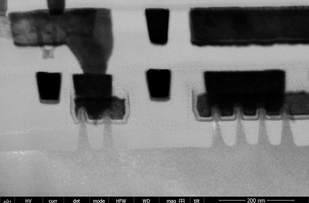
To better serve this market segment, Spirit has added a focused ion beam (FIB) and scanning transmission electron microscopy (STEM) capabilities. Rather than performing a mechanical cross-section (which involves polishing an entire integrated circuit until enough material has been removed that the device of interest is visible), the FIB can be used to perform targeted micro-sections, lifting out areas of the device only a few microns wide for analysis. These micro-sections are then imaged using STEM, which can provide the sub-nanometer resolution necessary to resolve even the most cutting-edge devices (the image above is of a 22-nanometer tri-gate process, Intel’s solution to the challenges posed by the process shrinks beyond the 32-nanometer node).
STEM must be performed on exceptionally thin samples (for best resolution, samples must be 100 nanometers thick or less); a byproduct of working with such thin samples is increased spatial resolution for elemental analysis tools like energy dispersive spectroscopy since the size of the sample provides a natural limit on the interaction volume of the electron beam. As a result, not only can very thin layers be imaged with higher clarity, but their composition can also be analyzed.
Reverse Engineering to Replace Legacy Components
Intellectual property analysis does not always mean diving into a sample in order to determine whether there is evidence of patent infringement. There are vast segments of the industry that rely on obsolete or legacy electronic components, due to the extensive characterization history available. Many of these old electronic devices are no longer supported by their original manufacturer; that said, the demand for these components is still present.
There are a limited number of solutions for engineers who need to source these obsolete components. They may turn to third-party suppliers and the “grey market”, where they have no guarantee of a component’s remaining lifespan or authenticity. Others may choose to reverse engineer the device and have it manufactured by another foundry.
Using SEM Mosaics to Reverse Engineer Electronic Device Layout and Schematics
In order to reverse engineer such a component, an engineer must be able to capture the layout and schematic of a device. SEM mosaics, an electron microscopy service offered at Spirit, provides a significant portion of the data needed to do electronics reverse engineering. By creating high-resolution, large area composite images of functional blocks (or, in some cases, entire die), it is possible to grab the floor plan of a device with minimal engineering interaction.
In some cases, these composite images can even be used as the input to specialized image recognition software that converts the images directly into GDSII layout files, cutting down immensely on the amount of engineering time necessary to recover an obsolete IC (integrated circuit).
Summary of Electron Microscopy Services
Electron microscopy services can provide key data for many types of intellectual property analysis; patent research, reverse engineering, and many others benefit from the rapid, high-resolution imaging and compositional analysis techniques made possible by the electron microscope. As technology continues to push the boundaries of size, creating smaller and smaller features, electron microscopy will only continue to grow in value.


