Every IC defects and failures analysis project is unique; rarely, if ever, will an analyst come across a defect that is exactly identical to one found on a previous project. The wide range of process types, device applications, and conditions that contribute to failure will change from device to device; since every defect is shaped by the circumstances surrounding its inevitable end of life, no two failures will be alike.
Although the specific circumstances of failure may be one-of-a-kind, most IC defects still fall within one of several different categories. These categories are not just convenient pigeonholes for describing a failure – in many cases, they help to indicate the proper course of analysis for the device.
Most Common Types of IC Defects and Failures
Probably the most common of all IC defects and failures are those related to electrical overstress, or EOS. Electrical overstress is the result of exposing a device to voltage and current levels far beyond those that the device is designed to withstand. This exposure may be accidental (due to transient effects, like electrostatic discharge, motor flyback, power surges, etc.) or negligent (a device being used in an unintended application, with a higher duty cycle or supply voltage than the device was designed for) – in either case, the result is an excess of electrical energy applied to the device, which gives out under the stress (sometimes spectacularly so).
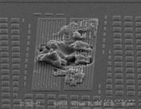
In the most exaggerated IC defects and failures cases, electrical overstress can transform a highly sophisticated integrated circuit into a slug of molten silicon slag. Generally speaking, however, the damage will be much more localized and difficult to find, requiring advanced analytical techniques to locate.
Current Leakage is a Telltale Sign of IC Overstress
IC devices that have been subjected to electrical overstress will exhibit current leakage when tested electrically; the excessive current traveling through the device is often the key to allowing an analyst to find the defect, generating heat, photons of light, and other phenomena that can be isolated using the precise tools and techniques of a failure analyst’s arsenal.
IC Overstress and Find Root Cause
Unfortunately, it is often difficult to determine the root cause of an electrical overstress event; the violent nature of EOS often consumes any pre-existing defect in the conflagration of arcing electricity and vaporizing metal (known to many engineers as “letting the smoke out” – since, naturally, all integrated circuits run on magic smoke, allowing the smoke to escape spells doom for a device). Even though the electrical overstress event often causes such severe damage that it is difficult to determine where the defect may have originated, a finding of EOS may still be useful for a customer evaluating a new product since it implies that there may be an inherent susceptibility to transients or improperly regulated power supplies.
Another common failure mode is an open circuit condition. Though an open circuit may be caused by electrical overstress, fusing bond wires, and metal traces, there are often more likely culprits. ICs and other devices exhibiting open circuits that are fresh from fabrication often exhibit processing defects, and failures resulting from improper manufacturing. These types of defects can take many forms: scratches on the surface of a die, left behind by probes during die or wafer testing, improperly etched metal traces, and poorly connected wire bonding are all examples of processing defects that are disastrous for product yield.
Some IC defects and failures may be even more difficult to pinpoint, like improperly drilled vias between metal layers, or misalignment of one layer of the die to the next – since these operations have extremely tight tolerances (in many cases, on the order of hundreds of nanometers), they can be exceptionally difficult to pinpoint using traditional inspection techniques.
Processing IC Defects and Failures
Processing defects are a far greater concern to a manufacturer than electrical overstress since they imply that there is an inherent process weakness with some (or all) of the devices produced in a certain time frame – often representing a huge loss in sales revenue, if the devices cannot be somehow verified as reliable enough for sale.
Many manufacturers will perform thorough qualification of any questionable product after failure analysis has uncovered a potential processing defect, in an effort to triage any product that may still be suitable for sale to try and recoup costs. That said, processing defects are not the only thing that could account for open circuits; often, after a long life in the field, a device may fail with an open circuit, simply due to device wear out – just like a car will eventually run itself into the ground, integrated circuits will eventually breathe their last gasp and fall silent. This may simply be due to the device’s normal lifespan, or it may be due to an inherent process weakness causing early life failures.
Finding open circuits can be a challenge since many of the tools used to find current leakage are completely impractical for locating an open (for example, a device that does not dissipate any power due to an open circuit will not heat up – making thermal imaging futile). Instead, other techniques – voltage contrast in an electron microscope, or time domain reflectometry – may be used as an alternative.
Though these may be the most common types of IC defects and failures, by no means is this list exhaustive – parts may fail in any of a number of different ways not explored here. The value of good failure analysis is the ability to determine the specific circumstances and characteristics of a given defect – while generalization may help to draw some conclusions about a failure, the devil is truly in the details when it comes to defects in integrated circuits.


