Over the course of a failure analyst’s career, they will be exposed to an extensive and varied array of devices. No matter the technology – whether they be nanoscopic silicon sensors with moving parts so small as to defy belief or massive circuit assemblies comprised of thousands of discrete components and integrated circuits – no device is completely immune to failure. Variations in process control, insufficiently robust designs and extended abuse by an end user can all spell early doom for a device. In our introductory article, we took a high-level overview of the failure analysis process, discussing the steps an analyst takes to turn a failing, rejected product into actionable knowledge for process improvement; in this column, we will see how these steps are applied to a specific failure. Naturally, examining a relatively trivial case would not provide the necessary depth of learning, so instead, we choose to give an example of a failure many analysts dread: an intermittent failure on a printed circuit assembly.
In this study, a single printed circuit assembly was received as an RMA from an end user. The end user was able to identify the failing assembly only by swapping parts; lacking any sort of test equipment, the customer was unable to provide any detail that could help to narrow the scope of the analysis beyond the most basic of failure descriptions (“this part doesn’t work anymore”). The first step in the failure analysis process is to verify the failure; after initial photo documentation, the assembly was put into functional testing using an application test bench. Initial results were disheartening, to say the least; the assembly functioned as designed, with supply current and output levels within specifications. In the absence of any reproducible failure mode, an analyst must rack their brain, grasping at any explanation for why the product has miraculously returned to normal function. Could the product have been improperly used by the customer – for example, were all connectors fully seated? Were power supply voltages stable and held at the correct levels? Had this board been processed with a top secret, self-healing material pulled straight from the annals of science fiction that had repaired whatever defect was responsible for the initial failure (hopefully not, lest our intrepid analyst find himself out of a job)? Fortunately, in this case, our analyst was rescued from the throes of despair and his search for a new career writing schlocky novellas about autonomous, regenerating electronic assemblies by a sudden change in the functional test results: an output that was previously within specifications suddenly dropped out, with only a fraction of the expected current being supplied to its load. Though our analyst rejoiced at being returned firmly to the realm of reality, these results indicated that the most likely root cause of failure would be hard to pin down – an intermittent connection.
The initial functional test led to several key observations that helped to characterize the failure. Initially, the assembly worked as intended, but after some period of time under power, the device would fail. Furthermore, the failure was not a “hard fail” (i.e. a short circuit or open circuit); power was still being supplied to the output pin, but insufficient drive current was available. After repeating the functional test and seeing the same failure characteristics, it was hypothesized that some thermal effect (thermal expansion, for example) was causing the device to fail. When first powered up, the board was at room temperature; however, after being under bias for a length of time, the power dissipated by the board caused enough self-heating to create a failure. Environmental testing was performed, and the temperature of the board was modulated; a strong correlation was noted between higher board temperature and reduced load current provided by the failing output. With the failure verified and characterized, the next step was to isolate the problem; in this case, isolation was done completely non-destructively, by tracing the circuit from the failing output back until an unexpected high resistance (48,000 ohms) between two points on the same node was noted.
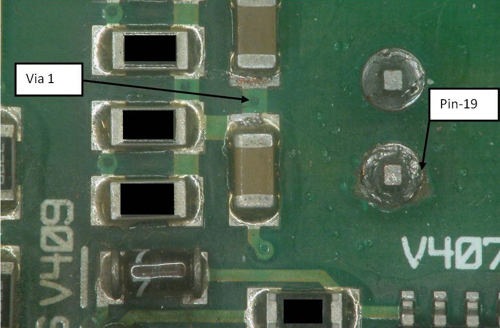
With the failure verified and isolated to a relatively small area, non-destructive testing procedures were performed. For PCB failures, x-ray analysis and optical inspection are chief among the non-destructive approaches available; other techniques, like acoustic microscopy, are more appropriate for component-level failures. At this point in the process, an analyst would inspect for cracked solder joints or broken PCB traces, misaligned via drills, or any other anomalous features that might help to explain the failure mechanism; in this particular case, no issues were noted during non-destructive testing. While a negative result like this may seem like no value added to the analysis, in this case, the data can be used to rule out certain types of defects (for example, a crack in the copper trace between the two points as a result of the warping of the PCB is unlikely).


