Continued from Failure Is The First Step on the Road To Success, Part 1
Non-destructive testing overlaps to a certain degree with the next step in the process, wherein an analyst attempts to isolate the failure to as small of an area as possible. This phase of the project may include both destructive and non-destructive aspects as necessary to locate a defect site. Some problems may be fairly simple to isolate, given the correct tools; a low resistance short between nodes of a board may be revealed in a matter of seconds using a thermal imaging camera, and the aforementioned cracked solder joint found during visual inspection can usually be probed for continuity with very little trouble. Other defects may require patience, a steady hand, and a methodical plan of attack; finding a leakage site on a PCB, for example, may require an analyst to cut traces (both on the surface of the PCB and buried within) in order to limit the number of possible locations for a defect.
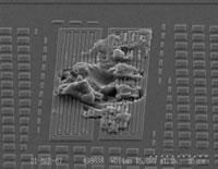
Once a potential defect site has been isolated, an analyst must be able to reveal the defect in all its glory. While the data gathered from isolation and non-destructive testing may be fairly strong, failure analysis follows the old clichés that “seeing is believing” and “a picture is worth a thousand words”; a failure analysis project is not truly finished until the analyst can produce images clearly showing a defect, removing any shadow of doubt that the anomaly found is at the heart of the reported problem.
This step is almost always destructive; the analyst must figuratively speaking, tear away the veil of FR4 and copper shielding the defect from view in order to definitively show the defect. At the assembly level, this often includes cross-sectioning (to show cracked vias and solder joints, or defects between PCB layers) or PCB delayering (to reveal damaged traces and voided or burnt dielectrics). Once the defect has been uncovered, an appropriate imaging solution can be chosen depending on the nature of the defect: high resolution optical or electron microscopes are sufficient for physical damage and defects, while tools like energy dispersive spectroscopy may be used to provide an “image” of contamination on a device that led to its early failure. With images in hand, an analyst’s work is almost finished.
In the final phase of a failure analysis project, an analyst must report their findings. The tools and techniques used by a failure analyst may not be familiar to their audience, who may be specialists in PCB assembly, metallurgy, or other disciplines. In some cases, the final audience of the report may be predisposed to disbelieve the results of an analysis (for example, in the case where the evidence shows that a subcontractor’s PCB’s do not meet required specifications, obligating them to re-run one or more lots of product). The failure analysis report must, therefore, be a clear, objective distillation of all data obtained during the course of the analysis, with a strong conclusion grounded in the facts revealed during the process. Whether the results point to a pervasive problem that must be remedied in order to meet reliability targets or are simply indicative of improper use by an end user, it is important to remember that the purpose of failure analysis is continuous improvement, not finger-pointing. Assigning blame does not offer a solution to a given problem; by understanding the nature of device failures, it is possible to implement corrective action (if necessary) to prevent recurrence of the same defect in future devices.
By following through the various steps of the failure analysis process – verification, NDT, isolation, revelation, and reporting – it is possible to take a device that would have been relegated to the trash can and transform it into a vital learning tool. It has been said that failure is the first step on the road to success; understanding the reason why a device has failed is a key starting point to creating a better device. Whether a defect was introduced during PCB manufacturing, solder reflow, or by an end user, all parties involved may learn from the anomaly and work to improve their own processes. While this article only provided a generic overview of the failure analysis flow, future articles will dive into further detail, exploring case studies that show the impact that failure analysis can have as well as exploring the techniques that go into a successful investigation. Until then, remember the motto of one of the most beloved groups of television scientists around – “Failure is always an option” – and keep an open mind to what that malfunctioning PCA might really be telling you!