FTIR Services in the Electronics Failure Analysis Lab

Spirit Electronics offers Fourier Transform InfraRed spectroscopy, or FTIR services when performing root cause analysis on the failure of an electronic component.

What is Fourier Transform Infrared?

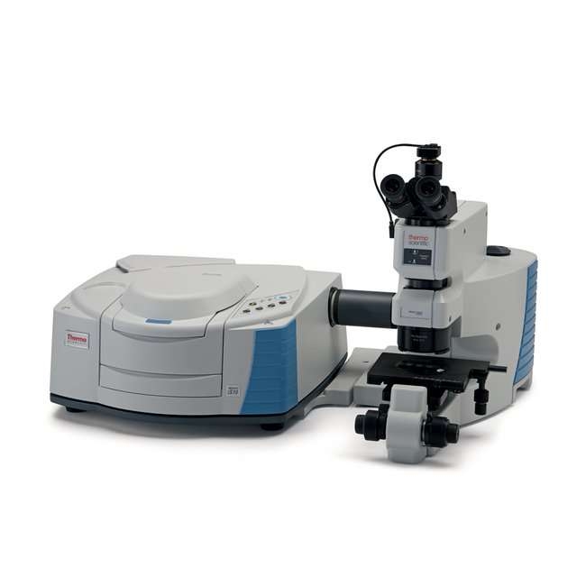
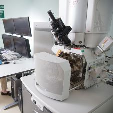
Fourier Transform Infrared analysis, also commonly referred to as FTIR Spectroscopy,  is a complex piece of scientific equipment used in our electronics failure analysis lab to scan material samples and observe chemical properties.  We use the FTIR scanning microscope to determine the chemical composition of organic materials, such as oils, fluxes, polymers, and in some cases inorganic materials.

How Does FITR Services for Electronic Failure Analysis Work?

The FTIR scanning microscope sends infrared radiation of about 10,000 to 100 cm-1 through an electronic component or material upon which the engineers in our microelectronics failure analysis lab are performing root cause analysis of failure.  Some of the radiation is absorbed and some pass through.

The radiation which is absorbed is converted into vibrational and/or rotational energy by the sample molecules. A signal is detected and represented as an IR spectrum, effectively providing a “fingerprint” of the material as the IR light is either absorbed or reflected.

The name Fourier-transform infrared spectroscopy is derived from the mathematical process known as a Fourier transform which is used to convert the raw data into the spectrum.

How Does Our Electronics Failure Analysis Lab Use the Fourier Transform Infrared?

FTIR spectroscopy is a well-established analytical technique used in our electronics failure analysis lab when evaluating manufactured electronics material. Our failure analysis engineers often use FTIR spectroscopy as the first step in the electronics failure analysis process.

The IR spectrum fingerprint can then be run against a database of over 50,000 organic materials, much like facial recognition programs seen on many law enforcement television shows. Samples can be as small as 10×10 square microns (a micron is a millionth of a meter, about a tenth the diameter of a hair).

So FTIR services are essentially a method of measuring infrared absorption and emission. We use FTIR spectroscopy in our electronics failure analysis lab to:

  • Recognize and define unknown materials
  • Find and identify contamination on or in a material
  • Perform failure analysis investigations to isolate oxidation, decomposition, and other causes of failing electronic components.

Semiconductor Failure Analysis Techniques

Semiconductor Failure Analysis – Enhancing Reliability

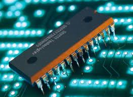
Semiconductor failure analysis occupies a prominent position among high-tech fabricators. Even the most sophisticated ICs fail, and when they do, it’s critical that engineers and fabricators discover the root causes of the failure, so as to avoid the same issues in subsequent designs.

Semiconductor analysis can, therefore, enhance semiconductor reliability by addressing observed shortcomings in design and fabrication and then avoiding them in the future.

Semiconductor failure analysis initially involves pinpointing the nature of the failure. Semiconductor failures can be broadly grouped into two categories: functional failures and parametric failures. A functional failure means the device failed in its intended function, while parametric failures mean the device’s function lies outside the specifications for a measurable characteristic.

Parametric failures have nothing to do with the intended functionality of the device. The initial phase of semiconductor failure analysis then calls for failure verification in which the failure is identified and categorized.

The next phase of testing seeks to localize the exact origin and causes of the failure. To achieve that goal, semiconductor failure analysis will subject the device to various forms of testing, some non-destructive, and others destructive.

Obviously, one must exercise caution in moving on to the destructive semiconductor failure analysis techniques, as they will render any other forms of testing impracticable. Some of the non-destructive semiconductor failure analysis techniques include optical microscopy, X-ray radiography, curve tracing and hermeticity testing. Destructive techniques include decapsulation, sectioning, microprobing, SIMS, LIMS and chromatography.

Together, these techniques will enable analysts to pinpoint the location and nature of the semiconductor failure. However, care must be taken to compare the results of various semiconductor failure analysis techniques to eliminate faulty conclusions based on conflicting results. Reliable semiconductor failure analysis requires careful examination by skillful engineers and not just the latest equipment.

Common Types of IC Defects and Failures

Every IC defects and failures analysis project is unique; rarely, if ever, will an analyst come across a defect that is exactly identical to one found on a previous project. The wide range of process types, device applications, and conditions that contribute to failure will change from device to device; since every defect is shaped by the circumstances surrounding its inevitable end of life, no two failures will be alike.

Although the specific circumstances of failure may be one-of-a-kind, most IC defects still fall within one of several different categories. These categories are not just convenient pigeonholes for describing a failure – in many cases, they help to indicate the proper course of analysis for the device.

Most Common Types of IC Defects and Failures

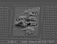
Probably the most common of all IC defects and failures are those related to electrical overstress, or EOS. Electrical overstress is the result of exposing a device to voltage and current levels far beyond those that the device is designed to withstand. This exposure may be accidental (due to transient effects, like electrostatic discharge, motor flyback, power surges, etc.) or negligent (a device being used in an unintended application, with a higher duty cycle or supply voltage than the device was designed for) – in either case, the result is an excess of electrical energy applied to the device, which gives out under the stress (sometimes spectacularly so).

In the most exaggerated IC defects and failures cases, electrical overstress can transform a highly sophisticated integrated circuit into a slug of molten silicon slag. Generally speaking, however, the damage will be much more localized and difficult to find, requiring advanced analytical techniques to locate.

Current Leakage is a Telltale Sign of IC Overstress

IC devices that have been subjected to electrical overstress will exhibit current leakage when tested electrically; the excessive current traveling through the device is often the key to allowing an analyst to find the defect, generating heat, photons of light, and other phenomena that can be isolated using the precise tools and techniques of a failure analyst’s arsenal.

IC Overstress and Find Root Cause

Unfortunately, it is often difficult to determine the root cause of an electrical overstress event; the violent nature of EOS often consumes any pre-existing defect in the conflagration of arcing electricity and vaporizing metal (known to many engineers as “letting the smoke out” – since, naturally, all integrated circuits run on magic smoke, allowing the smoke to escape spells doom for a device). Even though the electrical overstress event often causes such severe damage that it is difficult to determine where the defect may have originated, a finding of EOS may still be useful for a customer evaluating a new product since it implies that there may be an inherent susceptibility to transients or improperly regulated power supplies.

Another common failure mode is an open circuit condition. Though an open circuit may be caused by electrical overstress, fusing bond wires, and metal traces, there are often more likely culprits. ICs and other devices exhibiting open circuits that are fresh from fabrication often exhibit processing defects, and failures resulting from improper manufacturing. These types of defects can take many forms: scratches on the surface of a die, left behind by probes during die or wafer testing, improperly etched metal traces, and poorly connected wire bonding are all examples of processing defects that are disastrous for product yield.

Some IC defects and failures may be even more difficult to pinpoint, like improperly drilled vias between metal layers, or misalignment of one layer of the die to the next – since these operations have extremely tight tolerances (in many cases, on the order of hundreds of nanometers), they can be exceptionally difficult to pinpoint using traditional inspection techniques.

Processing IC Defects and Failures

Processing defects are a far greater concern to a manufacturer than electrical overstress since they imply that there is an inherent process weakness with some (or all) of the devices produced in a certain time frame – often representing a huge loss in sales revenue, if the devices cannot be somehow verified as reliable enough for sale.

Many manufacturers will perform thorough qualification of any questionable product after failure analysis has uncovered a potential processing defect, in an effort to triage any product that may still be suitable for sale to try and recoup costs. That said, processing defects are not the only thing that could account for open circuits; often, after a long life in the field, a device may fail with an open circuit, simply due to device wear out – just like a car will eventually run itself into the ground, integrated circuits will eventually breathe their last gasp and fall silent. This may simply be due to the device’s normal lifespan, or it may be due to an inherent process weakness causing early life failures.

Finding open circuits can be a challenge since many of the tools used to find current leakage are completely impractical for locating an open (for example, a device that does not dissipate any power due to an open circuit will not heat up – making thermal imaging futile). Instead, other techniques – voltage contrast in an electron microscope, or time domain reflectometry – may be used as an alternative.

Though these may be the most common types of IC defects and failures, by no means is this list exhaustive – parts may fail in any of a number of different ways not explored here. The value of good failure analysis is the ability to determine the specific circumstances and characteristics of a given defect – while generalization may help to draw some conclusions about a failure, the devil is truly in the details when it comes to defects in integrated circuits.

Avoid Electronic Failures with (EDS) Energy Dispersive Spectroscopy

Energy Dispersive Spectroscopy is like getting a fingerprint on your electronic component failure root cause.

So you’re having a problem with a printed circuit board assembly (PCBA). You’ve done all you can to narrow down the failure site, but you’re at the limit of the capabilities your equipment has available to you. What do you do now?

You see it, there’s something on your assembly that shouldn’t be there. Maybe it’s only one return that has the problem. If it’s a household product, you can probably ignore it. But if it’s in a critical market (aerospace, medical, automotive, etc.), your customer wants to know what it is, and how you’re going to prevent it from occurring again.

Or it could be that you’ve seen several of these failures recently and you need to know the level of your company’s exposure/risk or your customer is demanding immediate containment and a long-term fix.

Diagnosing the Problem Using Energy Dispersive Spectroscopy

With EDS (Energy Dispersive Spectroscopy) you can determine if the contaminant is organic or not, and what elements are present. This in itself can often help point to the source of the problem, but it’s an organic material, you should continue with the analysis using FTIR (Fourier Transform InfraRed).

By submitting the sample to a spectrum of the IR band and monitoring the frequencies that are absorbed and those that are reflected, a “fingerprint” of the sample can be obtained.

This technique has been around for decades and a vast library of “fingerprints” has been collected. An electronic failure analysis lab will have access to this library and can match your sample’s fingerprint to it. Thereby, determining its chemical composition.

Suppose it comes back as a flux, but your company uses three different types of fluxes. By submitting samples of the three fluxes to an electronic failure analysis company, their fingerprints can be compared to the original sample and the culprit identified.

You now possess the data you need to resolve the issue successfully. As a bonus, any good failure analysis report will provide the logical step-by-step details to support your conclusion, leading your customer to the same conclusion you arrived at.

Using a well-reputed third-party lab gives your customer confidence in the analysis because the data is unbiased.

Microelectronics X-Ray Imaging – Seeing Through to the Root of Failure

Microelectronics X-Ray imaging allows an analyst to see the inner workings of a device without disturbing its physical integrity.

What is Microelectronics X-Ray Imaging

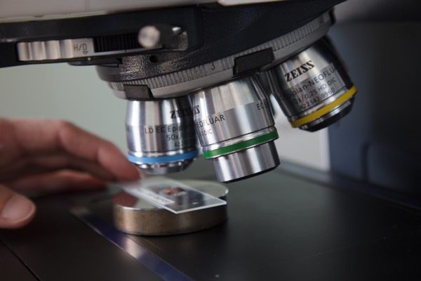
Most modern electronic devices are packaged as proverbial “black boxes.” It is nearly impossible to tell what is happening inside a device by looking at the outside packaging. What’s more, many devices are designed to be virtually impossible to open without causing irreversible changes to the product.

These types of electronic devices pose a unique problem for a microelectronics failure analysis lab – without being able to see the functional pieces of a device, it is nearly impossible to find a failing component or signal.

X-Ray Imaging Can See Without Destroying

While there are a plethora of destructive techniques available, allowing the analyst access to the “guts” of an electronic device, these techniques often carry with them a certain level of risk; destructively opening an integrated circuit or another assembly can, in very rare cases, induce damage.

To help prove beyond reasonable doubt that any damage an analyst finds was pre-existing and not created during the course of the analysis, a non-destructive way of looking inside the black box is necessary. X-Ray imaging lends itself perfectly to this application, penetrating the shroud surrounding most devices with ease.

X-Ray Imaging for Failure Analysis

The x-ray imaging systems used for failure analysis work in much the same way as those used for medical procedures, albeit at a much lower power level. By using an x-ray source and detector, an analyst can study the internal structure of a device to look for defects in the same way a doctor might study an x-ray to look for fractured bones.

Depending on the type of device and the reported failure condition, microelectronic x-ray imaging may be used to look for many different things. When studying an integrated circuit, for example, the x-ray can easily reveal problems with bond wires or flip-chip bumps, often showing open-circuit or short-circuit conditions and eliminating the need to open the package at all. Indeed, in some cases – for example, in the case of adjacent bond wires touching due to wire sweep during packaging – traditional decapsulation of the device can remove any evidence of the failure altogether!

X-ray imaging can also be useful for failure analysis of printed circuit assemblies. Since most modern circuit boards use multiple layers of conductive traces to route signals from point to point, it is not always possible to visually trace the electrical path between components. Since the x-ray can reveal all layers of a board simultaneously, following a signal and pinpointing a failure site is much more straightforward. Furthermore, some defects that may not be evident on visual inspection, like improper via drilling or component misregistration, can be identified much more readily with x-ray imaging.

Summary

Non-destructive testing (NDT) – gathering data about a sample without causing any irreversible harm or change – is one of the most important steps of failure analysis. By allowing an analyst to study the internal machinations of a sample without disturbing its physical integrity, x-ray imaging is an integral part of the NDT process.

Using FIB for Wafer Lot Acceptance and Design Verification

In this post, you will learn how an electronics failure analysis lab uses a FIB for Wafer Lot Acceptance during design verification.

In the current era of System-on-Chip (SoC) designs with 10 and 11 metal layers, copper metallizations, exotic dielectric materials, and the use of area pads scattered across the entire die area of circuit design, FIB provides an ideal diagnostic aid.

Using a FIB for Wafer Lot Acceptance

FIB (Focused Ion Beam) technology has certainly come a long way since its introduction in 1975. I recall very well the first encounter I had with the technology as a young ASIC designer in the late 80s. It seemed the most magical thing I had ever encountered: the ability to rework semiconductor devices, not only by being able to cut metallization lines (to correct shorts, for example, as had been done previously on a mechanical probe station), but also to add new conductive paths. FIB literally provided a designer the ability to add what are essentially blue wires to correct bugs in a design, as could be done with a board-level product. FIB truly opened a whole new world.

A Little FIB History

In the early days, FIB machines were cantankerous and required a tremendous level of skill and dedication to keep alive. The handful of good operators that existed was highly sought after and comprised something of a brotherhood of alchemists. The chamber size on the early machines was small, the ability to image was limited and the control of the beam for cutting and deposition was somewhat crude, with manual control over the beam’s raster pattern provided by physical potentiometers.

I spent many hours in the company of one of those alchemists staring at the flickering green phosphor screen on an early Seiko FIB machine, looking for the telltale image bloom and screen washout that would occur when cutting through interlayer dielectrics and into the next conductive layer. And lo and behold: after a few hours of work, the prototype IC that was stillborn due to an error that I had made sprang to life. Magic!

With later generations of FIB hardware, it became possible to integrate voltage-contrast microscopy with the milling and deposition process, and the integration of tester hardware allowed devices to be actually operated upon while running test vectors under normal operating conditions. Further development allowed the integration of the physical design database for the device into the navigation process, even allowing a specific node to be identified by name from a netlist, navigated to via the design database, imaged via voltage contrast, and then altered via FIB cuts or depositions- all in a single action.

This proved to be the designer’s best secret weapon for rapid debug and prototype bringup.

More than one design manager was heard to denigrate the benefits of FIB, stating that it made it “too easy to recover from mistakes that should never have been made in the first place”. However, FIB unquestionably saved the bacon of many a fallible designer, and its use has become commonplace.

Benefits of Using a FIB

The capabilities of modern FIB machines utterly overshadow the primitive capabilities I so revered from the 80s. In the current era of System-on-Chip (SoC) designs with 10 and 11 metal layers, copper metallization, exotic dielectric materials, and the use of area pads scattered across the entire die area of a design, FIB provides an ideal diagnostic aid. It is even now possible to perform “backside FIB”, which involves milling into the die from the substrate side (as opposed to the top metal/passivation side). This allows the operator to avoid having to cut through multiple metal layers and complex, dense routing structures, and approach active devices from below.

Taken as a whole, these capabilities have proven to be a major boon for electronic failure analysis processes. FA professionals can use the surgical precision afforded by the ion beam milling process to selectively strip back layers of overburden to reach and image very fine structures suspected of causing yield problems, infant mortality, or electromigration issues.

Exotic technologies such as Silicon-on-Insulator or III-V semiconductors pose little difficulty for modern FIB hardware. Similarly, advanced three-dimensional technologies such as FinFET or GAA (Gate All Around, or nanowire) transistor designs are handled quite well by modern FIB machines. Imaging and milling deposition resolutions have comfortably kept pace with technology steppings down to critical dimensions on the order of tens of nanometers, and the ion beam milling process is very compatible with fragile 3D structures. The technology provides debugging and diagnostic tools that were utterly unimaginable just a decade ago.

More Reasons We Love Using the FIB

Insight Analytical Labs has built a sizable practice around its state-of-the-art FEI Dual-Beam Field Emission Scanning Electron Microscope (FESEM), which provides FESEM functionality combined with a high-resolution FIB capability in a single vacuum chamber. This unit allows IAL to section and image devices with resolutions down to 5nm. It can be used to prepare samples for transmission electron microscopy (TEM), and also incorporates a scanning TEM detector, allowing the capture of much higher resolution images than possible with SEM alone.

Further, the FESEM chamber is large enough to accept any packaged IC as well as wafers up to 6”, and its internal toolset allows many routine operations to take place entirely inside the chamber without breaking the vacuum. It can perform many of the sample preparation, sectioning, and imaging tasks required for Wafer Lot Acceptance or other Failure Analysis tasks in a single pump-down, saving a tremendous amount of time and expense.

Summary

Gone are the old pots on the front panel for beam control, replaced with a comprehensive software-driven user interface. However, I suspect that the operators still have a bit of the alchemist about them: notwithstanding any possible secret handshakes, they are still the wizards of debugging, bring up, and failure analysis in the brave new nanometer world. If it is small, expensive, exotic, and not functioning as it should: FIB can help.

IC Decapsulation – Exposing Semiconductor Devices for Analysis

IC decapsulation is the half art, half science process of breaking into integrated circuits to discover what defects might lie within.

IC Decapsulation Reveals Hidden Secrets

In their final, packaged form, many of the secrets of integrated circuits are concealed from an analyst looking to uncover a failure. While techniques like x-ray and acoustic microscopy can penetrate the shroud of the mold compound and FR4 that enfold the semiconductor die at the heart of a device and reveal some information, they rarely tell the whole story; to truly determine the root cause of failure, an analyst almost always needs to be able to examine the device directly.

This examination may take many forms – optical or electron microscopy may reveal a defect site, or elemental analysis tools may identify contaminants causing corrosion or other issues – so the techniques used to expose the semiconductor die must take into account the potential failure mechanisms that are most likely for any given device.

IC decapsulation is the process – part art, part science – of breaking in to these devices to discover what defects might lie within.

IC Decapsulation Techniques

The most common technique used when performing IC decapsulation for a semiconductor failure analysis company is a wet chemical process. The mold compound on many products is susceptible to being dissolved by highly concentrated acids; since the vast majority of the semiconductor die are protected by a passivation layer that is relatively impervious to these acids, there is little risk of damaging the device with this process, though a certain amount of care must be taken with unpassivated metals like aluminum bond pads to ensure they do not etch away along with the mold compound.

Some specialized failure analysis equipment will perform a wet decapsulation with pressurized streams of heated acid, focused by nonreactive gaskets onto the area of the IC package that an analyst wishes to remove. These IC decapsulation systems are limited by the selection of gaskets available to an analyst; without an appropriate gasket set, it is possible to either underexpose or overexpose the die, either of which can be problematic for further analysis.

Many analysts prefer a more hands-on, low-tech approach to wet decapsulation: the sample is heated, and acid is trickled onto the device, one drop at a time; the dissolved product is rinsed away with a solvent, eventually exposing the die. With practice and good technique, an analyst using this approach can expose the semiconductor die without impacting any leadframe or underlying circuitry, so the device will function (mostly) identically to how it performed before decapsulation, allowing the use of isolation techniques like thermal imaging or photoemission.

Though wet decapsulation is certainly the most common method, it is not appropriate for all types of semiconductor failure analysis. Contaminants on the surface of the semiconductor die can be washed away by the acids and solvents; if the contaminants had no secondary effect (for example, corrosion of the traces on the IC), there will often be no remaining clue as to the root cause of failure on the device.

IC Decapsulation When Contamination if Present

If something in the failure characteristics or device history suggests that contamination might be present, a different decapsulation approach is necessary. For plastic encapsulated devices, one such method is plasma etching. The sample is placed in a tool capable of generating a reactive plasma – a reactive ion etcher is the most likely candidate since the FA lab is likely to have one already to support deprocessing work – and exposed to pure oxygen gas. The plasma oxidizes the plastic mold compound, turning it into a fine ash that can be easily cleaned away, eventually revealing the die. Many contaminants that might lead to a failure – halides, metal particulate, and others – do not react with this oxygen plasma, or react at a much slower rate, and so are left behind by the ashing process.

The assumption in both wet IC decapsulation and plasma etching as described above is that a semiconductor is encased in a plastic mold compound; for devices in ceramic cases, embedded in other types of materials, or mounted in other unusual ways (for example, many mobile devices mount the semiconductor die as a flip-chip directly onto the printed circuit board, forgoing traditional packaging altogether), other techniques must be developed and deployed. A certain degree of creative latitude is necessary

Electron Microscopy Services for Intellectual Property (IP) Analysis

Electron microscopy services can provide key data for many types of intellectual property (IP) analysis including patent research, reverse engineering, and microelectronics IP infringement analysis, to name just a few. This post explores how electron microscopy supports electronics intellectual property analysis.

Today’s cutting-edge microelectronics are twisting, labyrinthine networks of nanotechnology, with layers upon layers of intertwined metallic and crystalline structures.

Gone are the days when one could put an electronic device under an optical microscope and, over the course of a few hours, sketch out a relatively accurate functional schematic; the process technology used in creating a modern microprocessor or memory device creates features so small that they are physically impossible to resolve with optical microscopy since the wavelength of visible light is so much larger than the features being imaged.

Higher-resolution electron microscopes can easily resolve the nanometer-scale features on these devices, but the ultra-high magnifications needed to do so mean that only very small areas of the die can be viewed at a given time, an equally restrictive roadblock to understanding a circuit as a whole.

Intellectual Property Analysis of Electronics

Performing intellectual property analysis on an electronic device in order to protect patents or reverse engineer obsolete electronic parts which are no longer manufactured is, in many cases, an exercise in competing compromises; one can get a highly focused analysis with electron microscopy that is very limited in scope, or a very broad look at a device that may lack the necessary depth for certain investigations.

Fortunately, Spirit is offering electron microscopy services that work to bridge the gap between viewing large areas and imaging at high resolution.

The Higher the Resolution the Better for Intellectual Property Analysis

When performing intellectual property analysis on electronics to determine whether or not there is patent infringement, it is often important to closely study the materials and processes used to construct a specific semiconductor, integrated circuit, or other devices.

The minutiae of how a transistor is formed can be crucial to the claims of a given electronic component patent. Traditionally mechanical cross-section and SEM inspections have been used to gather this data. However, these electronic reverse engineering techniques have limited precision and resolution, and are not ideal for differentiating very small constructions (for example, the layers of oxide and nitride used as tunneling barriers in memory cells).

Furthermore, a traditional mechanical section is not a good fit for performing elemental analysis of the layers of a device, as the interaction volume of the electron beam is so large that isolating individual layers to determine their composition is impossible.

FIB and STEM – Work Horses of IP Analysis

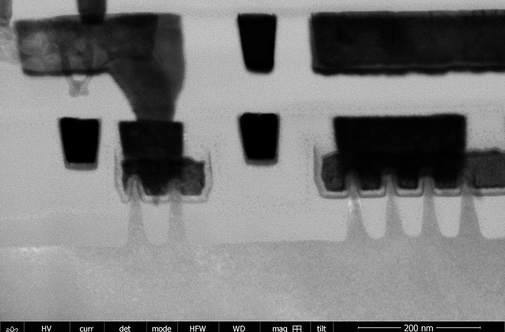
To better serve this market segment, Spirit has added a focused ion beam (FIB) and scanning transmission electron microscopy (STEM) capabilities. Rather than performing a mechanical cross-section (which involves polishing an entire integrated circuit until enough material has been removed that the device of interest is visible), the FIB can be used to perform targeted micro-sections, lifting out areas of the device only a few microns wide for analysis. These micro-sections are then imaged using STEM, which can provide the sub-nanometer resolution necessary to resolve even the most cutting-edge devices (the image above is of a 22-nanometer tri-gate process, Intel’s solution to the challenges posed by the process shrinks beyond the 32-nanometer node).

STEM must be performed on exceptionally thin samples (for best resolution, samples must be 100 nanometers thick or less); a byproduct of working with such thin samples is increased spatial resolution for elemental analysis tools like energy dispersive spectroscopy since the size of the sample provides a natural limit on the interaction volume of the electron beam. As a result, not only can very thin layers be imaged with higher clarity, but their composition can also be analyzed.

Reverse Engineering to Replace Legacy Components

Intellectual property analysis does not always mean diving into a sample in order to determine whether there is evidence of patent infringement. There are vast segments of the industry that rely on obsolete or legacy electronic components, due to the extensive characterization history available. Many of these old electronic devices are no longer supported by their original manufacturer; that said, the demand for these components is still present.

There are a limited number of solutions for engineers who need to source these obsolete components. They may turn to third-party suppliers and the “grey market”, where they have no guarantee of a component’s remaining lifespan or authenticity. Others may choose to reverse engineer the device and have it manufactured by another foundry.

Using SEM Mosaics to Reverse Engineer Electronic Device Layout and Schematics

In order to reverse engineer such a component, an engineer must be able to capture the layout and schematic of a device. SEM mosaics, an electron microscopy service offered at Spirit, provides a significant portion of the data needed to do electronics reverse engineering. By creating high-resolution, large area composite images of functional blocks (or, in some cases, entire die), it is possible to grab the floor plan of a device with minimal engineering interaction.

In some cases, these composite images can even be used as the input to specialized image recognition software that converts the images directly into GDSII layout files, cutting down immensely on the amount of engineering time necessary to recover an obsolete IC (integrated circuit).

Summary of Electron Microscopy Services

Electron microscopy services can provide key data for many types of intellectual property analysis; patent research, reverse engineering, and many others benefit from the rapid, high-resolution imaging and compositional analysis techniques made possible by the electron microscope. As technology continues to push the boundaries of size, creating smaller and smaller features, electron microscopy will only continue to grow in value.

What can Acoustic Microscopy do for you?

Analogy Time

Consider something like automobile production in the United States. It stands at about 12,000,000 cars per year. If 99.9% came off the assembly line in perfect condition and ready-to-drive that would look pretty good on paper.

Except, perhaps, for the large parking lot outside the assembly plant that would be required to store the bad cars; with 1/10th of 1% of the production failing, 12,000 bright, shiny, brand new cars would be sitting out in the lot. Better plan on having about 250 parking places ready at all times. At least the mechanics and technicians would have permanent jobs.

Microchips

Scanning Acoustic Microscopy labFor the average person looking at a tiny microchip, there’s very little to see. It’s a mysterious black box with “magic” inside. Show them a whole circuit board and suddenly they imagine an aerial view of a cityscape; a burgeoning metropolis with millions of residents and insane complexity. If you were to take a look inside a microchip, you would also see a city with roads of aluminum and copper busily running atop the surface of the silicon die, layer upon layer of them. They make the worst interstate exchange in LA look like a country road.

Integrated circuits (ICs) are extremely complex and would not exist as they do today if not the continued improvements in computers and software. Most ICs these days are packaged (molded) in an epoxy (the “black box” we see) that protects the IC while providing electrical paths from the IC to the outside world. Electrical testing of the ICs ensures they are functional before they’re shipped, but like all things in nature, they will degrade with time.

Although many of the causes of failure, the failure mechanisms, are associated with the IC itself, these failure mechanisms typically do not manifest themselves till much later (10-20 years or longer) in the IC’s lifetime. The packaging of the part though also introduces possible failure mechanisms, many of which will decrease the lifetime of the product to 1-3 years. These include voids in the epoxy (which lead to uneven stresses in the package), and delamination of the plastic to the IC die or the leadframe (which also causes uneven stresses within the package and can be an accumulation area for moisture or other contaminants.

Uneven stresses, or stress gradients, are fairly neutral at a constant ambient temperature, but when the device temperature increases (from self-heating and/or external temperature increases), the plastic encapsulant (the package) expands more than the IC die in the package. A uniform encapsulant will put uniform stress on the die, but if there is an area of delamination or a void over the IC die or a wire bond, it can lead to a cracked die or broken wire bond.

If the delamination is not over the die, it may be acceptable if it doesn’t extend to the outside of the package (which would let contaminants onto the die). When these types of delaminations exist, accelerated stress, such as temperature cycling, should be used to ensure delaminations do not “grow” and reach the exterior of the package.

In some surface-mount packages, delamination under the leadframe has been known to accumulate water vapor. During the soldering process to the board, this water vapor turns to steam, stressing the package to fracture. This is known as “popcorn cracking”. But which packages have a problem and which are good?

SAM to the Rescue

How does one prevent these package problems? First, process controls must be in place in the manufacturing line to ensure the process produces the same high-quality product each time. To check to see if the present product is free of these unacceptable flaws, Scanning Acoustic Microscopy (SAM) is utilized. While X-ray inspections image differences in a materials’ densities in a package, SAM uses sound waves to image the inside of the package. This is much like the use of ultrasounds in a hospital to imaging soft tissue (such as babies in the womb or hearts, which X-rays pass through without a clear image). As such, SAM is an excellent complement to X-rays and is considered non-destructive.

As part of an IC’s qualification, the package should be inspected for voids and delaminations in the package. SAM is normally performed on the first product produced providing a baseline for the device. After this initial testing, the samples are normally subjected to temperature cycles, and then SAM tested again to see if the baseline data changed. This cycle of Scanning Acoustic Microscopy inspections and temperature cycling is often repeated until the integrity of the package is demonstrated (or adversely, is shown to have a problem).

Since SAM systems rely on sound waves to collect the data about the inside of a package, the frequency of the sound wave plays an important role. High-frequency waves provide the most resolution, but cannot penetrate deep into the sample. Conversely, low-frequencies can penetrate even through the sample (through transmission) but do not afford the resolution of the high-frequency transducers. As such, the selection of the appropriate transducer will have a strong effect on the acoustic image and the information it provides.

There are different SAM manufacturers and models available and they all have their good points. Your choice depends on your needs. To continue the car analogy, one type doesn’t suit all—you don’t need a pickup truck to deliver jewelry, and you can’t use a Tesla to take five kids to soccer practice.

The Many Modes of SAM

If only naval sonar was as accurate as SAM! All the different scanning methods could provide insights that would otherwise be impossible to obtain. Of course, SAM is not the exclusive domain of the microelectronics industry.

The medical field has found uses for it to study biological cells and tissues for structure and motility. They have even used it to determine the efficacy of needle-less injections demonstrated by “Dr. Leonard McCoy” from the first Star Trek series way back in the 1960s. We actually have working models of that device now. Fascinating…

For our purposes, however, there are several very prevalent SAM modes and they reveal different aspects of problems. Typical modes that all the equipment vendors offer are:Scanning Acoustic Microscopy failure analysis

  • A-scan: The C-scan data is arranged versus a horizontal axis of time. This mode is very helpful in identifying the location of the void or delamination in a package.
  • B-scan: This is a cross-sectional view of the sample in a single plane.
  • C-scan: A 2-dimensional image created from the returned waveforms (pulse-echo mode) of the transducer.

Using an acoustic transducer, a wave front passes into the object of interest, which is typically in a water tank; the water couples the sound energy from the transducer to the sample. Variances in the sound conduction ability of the internal materials reflect the energy back to the transducer. Any “air gaps” in the package will reflect the entire sound wave, highlighting a potential problem. Anomalies are quickly identified and can be used for further studies and feedback to production.

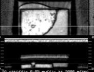
For example, the delaminations between the packaging and the chip are a must-know item, but knowing where they occur is equally important. Does it occur at the die/adhesive level (die attach) or the adhesive/leadframe level? An A-scan (much like a cross-section) reveals diagnostic detail not clearly shown by other methods. In the included acoustic image, the C-scan is shown on the top for reference, which shows an area of delamination. The white line is the point of the cross-section shown, the A-scan in the bottom half of the photograph. Clearly, there is delamination at the die/adhesive level, but it also occurs at the adhesive/leadframe. You must solve both problems or you solve neither!

Sonoscan C-SAM®

Consider the FACTS²™ DF2400™ C-SAM® (by SONOSCAN) unit which can image with a precision of ± 0.5 microns using multiple scan heads. It can improve in-production throughput between 2 and 7 times over earlier units. It can handle Auer Boat carriers, JEDEC trays or even IGBT modules.

If you’re using very small parts, an optional vacuum hold-down assures high-quality images. The waterfall/plume transducers eliminate immersion to prevent water ingress (if that is a concern), plus it eliminates “floating” for additional image quality. (Want to see it work? Click the caption under this image to see the DF2300™ in action).

Sonix SAM

Scanning Acoustic Microscopy manufacturesThis company has been busy innovating since 1986, and pioneering breakthroughs for accurate imaging; they’ve often led the industry by finding solutions that eluded others.

In a further example of an in-line, fully-automated scanner (by Sonix), we see that it offers similar capabilities to the Sonoscan C-SAM, but Sonix is particularly proud of its over-sampling, anti-aliasing capabilities. Aliasing occurs when there isn’t enough overlap on the readings such that images begin to look blocky. Fine detail can be lost, especially as components continue to diminish in size.

You may have experienced this with textures in video games, for example. This screen-grab obtained from a video game shows the effect of whether anti-aliasing technology is off (left half) or on (right half). The smoothing isn’t an artifact—it is an actual increase in detail—and that helps us spot problems.

With MUF (Molded Under-Fill) for flip-chips, you decrease manufacturing costs; however, the epoxy is not nearly as transparent as silicon and can have particles that give false positives to SAMs. Sonix’s MFCI™ software compensates for spatial and edge resolution, as well as enhancing contrast. If you were thinking that MUF was an artificial economy, it’s not—and Sonix may have your solution.

OKOS SAM

This company is comfortable dealing with NDT (nondestructive testing) on just about all of the semiconductor packages you can imagine, even wafers, motherboards, LED/LCD panels, flip-chips, or plastic packages. They too have exclusive software (called WinSam®), that works in combination with their special transducers and custom digitizers. They can handle just about every type of scan from “A” to “3D”.

They offer different models of SAMs such as the 250-P, whose smaller size is perfectly suited to laboratory work; the 400-P in-line model that will suit a production facility; or the granddaddy of them all, the Macrovue 1000. Complemented by their less bulky transducer/receivers, they significantly increase the scanning resolution capability for hybrid and other emerging technologies.

They even offer training refreshers for scanning techniques, starter classes for your team, or advanced training courses. You can contact them for training subjects offered, and pricing.

The Takeaway

There is no definitive winner in these, or any of the other models, available nowadays. It is so highly dependent on your own needs. Every unit will have its own niche. Your best choice is always to investigate with the manufacturers themselves.

Send them samples to be tested (usually for free!) to see what kind of results they can achieve for you. Let their skilled people put their own machines through their paces so you can see what the maximum capacity is. With appropriate training, whatever they can do, you can accomplish, too.

Or if you just have a now-and-then need, contact Spirit Electronics and talk to their experts about acoustic microscopy. They can run your samples and help interpret the data while providing quick turn times.

FIB Failure Analysis Services – Drilling Into The Core of Failure

Focused ion beam or FIB failure analysis services provide surgical precision when performing microelectronics root analysis.

The final step in the majority of integrated circuit failure analysis projects involves deprocessing the device, removing layers of metal and oxide to expose the defect on the device. Though the techniques of deprocessing are incredibly involved and require extremely high levels of skill, they are still inherently brute-force techniques, involving volatile chemicals and abrasive polishes.

In some cases, such an approach may be too aggressive. Fortunately, there are tools in an analyst’s repertoire that can be wielded with scalpel-like precision; using our arsenal of FIB failure analysis services allows an analyst to forgo lapping or wet etching in favor of drilling directly to the site of failure.

What does a FIB do?

A focused ion beam uses a precisely controlled stream of charged particles, similar to an electron microscope, to generate an image; unlike the electron microscope, however, the FIB uses a stream of gallium ions, which can also be used to ballistically etch material away from the surface of a device. Since this beam can be targeted so accurately (in some cases, within several nanometers), the site of a defect can be exposed without any disruption of the surrounding circuit. As a result, FIB failure analysis can often be performed more quickly and efficiently than through other methods.

FIB failure analysis services benefits

The inherent precision of the FIB also lends itself to performing “micro-surgery” on failing products, rewiring the device to allow minor changes to a device to examine its effects on the overall device functionality. In many cases, the first production run of a given product (often referred to as “first silicon”) will have performance issues arising from disconnects between modeling, simulation, and the real-world physics of the device.

Editing the design and making a new set of masks is often the only fix; however, the price of a new mask set can be exorbitant, especially considering that the new set of masks will often be nothing more than a test of a designer’s best calculation of the needed change.

Before shelling out the tens and hundreds of thousands of dollars for new masks, it is often prudent to take a handful of failing samples to the FIB, where traces can be cut and rewired by patterning conductive traces (usually made of tungsten or platinum) on the device. This allows for a quick, easy, and (most importantly) inexpensive test of any proposed design edits.

Summary

Of course, the FIB has many applications beyond FIB failure analysis. A FIB can be used to perform quick cross-sections of a device where the area of interest is relatively small; it can also be used to prepare samples for transmission electron microscopy, which requires extremely thin samples (less than 100 nanometers in many cases) to produce meaningful data.