Focused ion beam or FIB failure analysis services provide surgical precision when performing microelectronics root analysis.
The final step in the majority of integrated circuit failure analysis projects involves deprocessing the device, removing layers of metal and oxide to expose the defect on the device. Though the techniques of deprocessing are incredibly involved and require extremely high levels of skill, they are still inherently brute-force techniques, involving volatile chemicals and abrasive polishes.
In some cases, such an approach may be too aggressive. Fortunately, there are tools in an analyst’s repertoire that can be wielded with scalpel-like precision; using our arsenal of FIB failure analysis services allows an analyst to forgo lapping or wet etching in favor of drilling directly to the site of failure.
What does a FIB do?
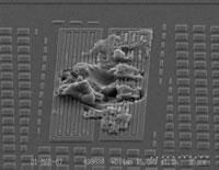
A focused ion beam uses a precisely controlled stream of charged particles, similar to an electron microscope, to generate an image; unlike the electron microscope, however, the FIB uses a stream of gallium ions, which can also be used to ballistically etch material away from the surface of a device. Since this beam can be targeted so accurately (in some cases, within several nanometers), the site of a defect can be exposed without any disruption of the surrounding circuit. As a result, FIB failure analysis can often be performed more quickly and efficiently than through other methods.
FIB failure analysis services benefits
The inherent precision of the FIB also lends itself to performing “micro-surgery” on failing products, rewiring the device to allow minor changes to a device to examine its effects on the overall device functionality. In many cases, the first production run of a given product (often referred to as “first silicon”) will have performance issues arising from disconnects between modeling, simulation, and the real-world physics of the device.
Editing the design and making a new set of masks is often the only fix; however, the price of a new mask set can be exorbitant, especially considering that the new set of masks will often be nothing more than a test of a designer’s best calculation of the needed change.
Before shelling out the tens and hundreds of thousands of dollars for new masks, it is often prudent to take a handful of failing samples to the FIB, where traces can be cut and rewired by patterning conductive traces (usually made of tungsten or platinum) on the device. This allows for a quick, easy, and (most importantly) inexpensive test of any proposed design edits.
Summary
Of course, the FIB has many applications beyond FIB failure analysis. A FIB can be used to perform quick cross-sections of a device where the area of interest is relatively small; it can also be used to prepare samples for transmission electron microscopy, which requires extremely thin samples (less than 100 nanometers in many cases) to produce meaningful data.